
Description
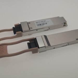
HD-QSFP+/40G-SR4 QSFP+ Optical Transceiver Module
| Optical Transmitter Characteristics | ||||||
| Parameter | Symbol | Min | Typical | Max | Unit | Notes |
| Center Wavelength | λout | 840 | 850 | 860 | nm | |
| Average Launch Power each
lane |
Pout | -7.6 | 2.4 | dBm | ||
| Difference in Power between
any two lanes [OMA] |
DPX | 4.0 | dB | |||
| Peak Power per Lane | PPX | 4.0 | dBm | |||
| Spectral Width (RMS) | σ | 0.65 | nm | |||
| Optical Extinction Ratio | ER | 3.0 | dB | |||
| Transmitter and Dispersion
Penalty each lane |
TDP | 3.5 | dB | |||
| Optical Return Loss Tolerance | ORL | 12 | dB | |||
| Average launch power of OFF
transmitter, per lane |
-30 | dBm | ||||
| Transmitter eye mask
definition{X1,X2,X3,Y1,Y2,Y3} |
{0.23,0.34,0.43,0.27,0.35,0.4} | |||||
| Optical Receiver Characteristics | ||||||
| Parameter | Symbol | Min | Typical | Max | Unit | Notes |
| Receiver Wavelength | λin | 840 | 860 | nm | ||
| Average Receive Power per
Lane |
RXPx | -9.5 | 2.4 | dBm | ||
| Stressed Receiver Sensitivity in
OMA |
SRS | -5.4 | dBm | 1 | ||
| LOS Assert | LOSA | -30 | dBm | |||
| LOS De-Assert | LOSD | -12 | dBm | |||
| LOS Hysteresis | 0.5 | dB | ||||
| Receiver Reflectance | Rfl | -12 | dB | |||
Notes:
1.Measured with a PRBS 231-1 test pattern, @10.3125Gb/s, BER<1E-12.
| Pin | Symbol | Name/Description | Notes |
| 1 | GND | Transmitter Ground | 1 |
| 2 | Tx2n | Transmitter Inverted Data Input | |
| 3 | Tx2p | Transmitter Non-Inverted Data output | |
| 4 | GND | Transmitter Ground | 1 |
| 5 | Tx4n | Transmitter Inverted Data Input | |
| 6 | Tx4p | Transmitter Non-Inverted Data output | |
| 7 | GND | Transmitter Ground | 1 |
| 8 | ModSelL | Module Select | |
| 9 | ResetL | Module Reset | |
| 10 | VccRx | 3.3V Power Supply Receiver | 2 |
| 11 | SCL | 2-Wire serial Interface Clock | |
| 12 | SDA | 2-Wire serial Interface Data | |
| 13 | GND | Receiver Ground | 1 |
| 14 | Rx3p | Receiver Non-Inverted Data Output | |
| 15 | Rx3n | Receiver Inverted Data Output | |
| 16 | GND | Receiver Ground | 1 |
| 17 | Rx1p | Receiver Non-Inverted Data Output | |
| 18 | Rx1n | Receiver Inverted Data Output | |
| 19 | GND | Receiver Ground | 1 |
| 20 | GND | Receiver Ground | 1 |
| 21 | Rx2n | Receiver Inverted Data Output | |
| 22 | Rx2p | Receiver Non-Inverted Data Output | |
| 23 | GND | Receiver Ground | 1 |
| 24 | Rx4n | Receiver Inverted Data Output | |
| 25 | Rx4p | Receiver Non-Inverted Data Output | |
| 26 | GND | Receiver Ground | 1 |
| 27 | ModPrsl | Module Present | |
| 28 | IntL | Interrupt | |
| 29 | VccTx | 3.3V power supply transmitter | 2 |
| 30 | Vcc1 | 3.3V power supply | 2 |
| 31 | LPMode | Low Power Mode,not connect | |
| 32 | GND | Transmitter Ground | 1 |
| 33 | Tx3p | Transmitter Non-Inverted Data Input | |
| 34 | Tx3n | Transmitter Inverted Data Output | |
| 35 | GND | Transmitter Ground | 1 |
| 36 | Tx1p | Transmitter Non-Inverted Data Input |
Notes:
1.GND is the symbol for signal and supply (power) common for the QSFP+ module. All are common within the QSFP+ module and all module voltages are referenced to this potential unless otherwise noted. Connect these directly to the host board signal-common ground plane.
2.Vcc Rx, Vcc1 and Vcc Tx are the receiver and transmitter power supplies and shall be applied concurrently. Requirements defined for the host side of the Host Edge Card Connector are listed in Table 6. Recommended host board power supply filtering is shown in Figures 3 and 4. Vcc Rx Vcc1 and Vcc Tx may be internally connected within the QSFP+ Module in any combination. The connector pins are each rated for a maximum current of 500 mA.

Figure 1.Electrical Pin-out Details
|
Part. No |
Specifications | ||||||||
|
Pack |
Rate* (Gbps) | Po (dBm) |
RX |
Sen* (dBm) | Temp (℃) | Reach (m) | Pull tap
Color |
DDM |
|
| HD-QSFP+/40G-SR4 | QSFP+ | 4*10.3125 | -7.6~2.4 | PIN | <-9.5 | 0~+70 | 150 | Beige | Y |
*Note:
- Measured with a PRBS 231-1 test pattern, @10.3125Gb/s, BER<1E-12. 2.Receiver sensitivity in OMA